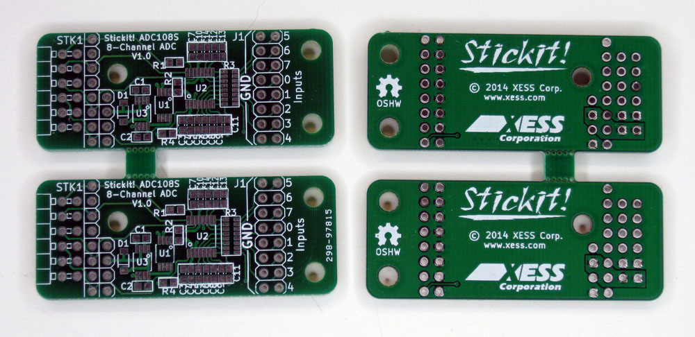
![]() I talked last time about my move to KiCad and the eight-channel analog-to-digital convertor (ADC) board I used for an initial test of the design software. I submitted the Gerber files to Itead on March 24th and received twenty-four PCBs on April 4th for a total charge of $14 USD.
I talked last time about my move to KiCad and the eight-channel analog-to-digital convertor (ADC) board I used for an initial test of the design software. I submitted the Gerber files to Itead on March 24th and received twenty-four PCBs on April 4th for a total charge of $14 USD.
The boards look good. (I had them fabbed as pairs since two PCBs would fit within the 2" x 2" panel that Itead allows.) The silkscreen is OK and the drill holes are pretty much in the center of the via pads. I couldn't see any shorts between the copper planes and the pads, and continuity tests confirmed this. (I used 8-mil trace/space, so I wasn't expecting any problems.) Overall, it looks like I correctly used KiCad to generate Gerber files that a PCB manufacturer could fabricate.
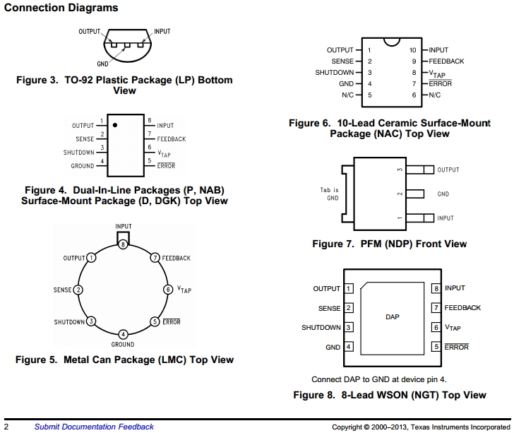
But would they work? With the PCBs in hand, it was time to build a test unit and see. I ordered some samples of the ICs I needed from Texas Instruments: the LM2660 voltage doubler, the LP2950 5V regulator, and the ADC108S102 eight-channel ADC. This was where I noticed my first mistake: the LP2950 is only available in a TO-92 package, not the MSOP-8 package I used for U1 on the PCB. In my haste, I had only given the following figure a cursory examination and just assumed all the regulators were offered in each package. That was so not true!
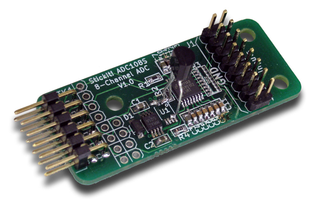
Since I didn't want to delay my test by re-fabbing the boards, I just ordered the LP2950 in the TO-92 package and stitched it onto the board as you can see below. (That was my second try at mounting the LP2950. In my first, I soldered it in backwards.) Applying 3.3V to the board, the LM2660 kicked it up to 6.6V and the LP2950 regulated that down to 5.0V with a tolerance of 0.5% for use as a reference by the ADC chip. So that seemed to be working.
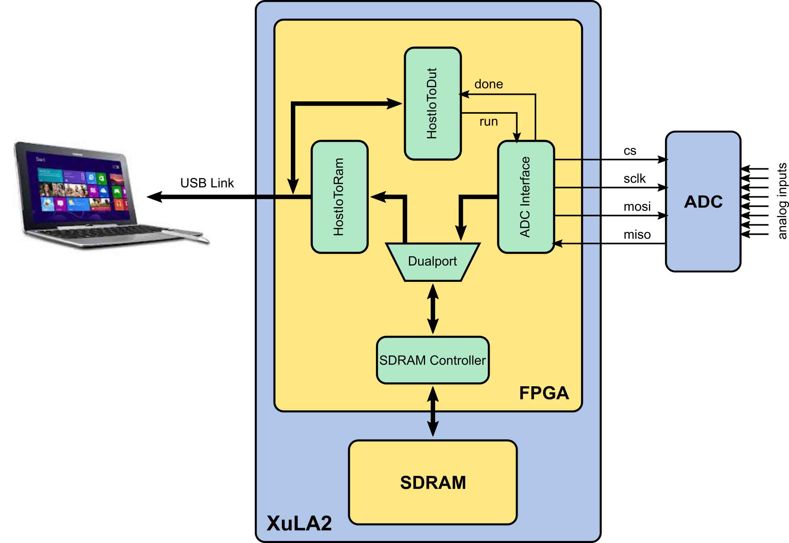
It wasn't possible to test much more of the board without configuring the FPGA with a circuit to read data from the ADC108S chip. To do that, I wrote some VHDL for a simple data sampler based on the architecture shown in the block diagram below. The ADC interface gets digitized samples of analog signals from the ADC board at a rate of 1 Msamples/second over an SPI communication bus. Each sample is written to the next free address location in the SDRAM of the XuLA2 board and then the address is incremented. The host PC can enable, disable and monitor a sampling run through the HostIoToDut interface. After a sampling run is completed, the PC uploads the samples from the SDRAM through the HostIoToRam interface.
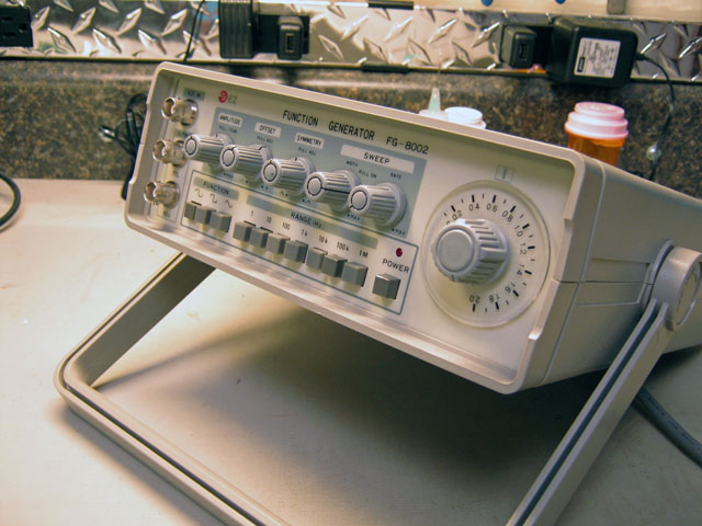 Now I had to find some way to apply waveforms to the ADC board and observe the results. The ADC board works with unipolar voltages between 0 and 5V. Unfortunately, my old signal generator only has a single bipolar output and the DC offset has stopped working, so it wasn't up to the task. Now what?
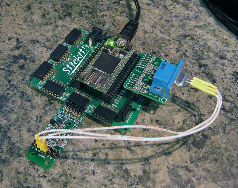
Well, with an FPGA, what you don't have you can build. To generate test signals, I augmented my FPGA design with three, independent sine-wave generators having individually-adjustable frequencies, amplitudes and DC-offsets. Then I could pump the digital outputs of the sine-wave generators into a StickIt! VGA board which has three digital-to-analog converters (DACs) that output analog signals in the range 0 to 3.3V. From there, it's a simple matter to connect the red, green and blue signals from the VGA connector to channels 0, 1 and 2 of the ADC board like so:
With the circuitry and FPGA design pretty much in hand, I turned my attention to the software that runs on the PC. I wrote a 50-line Python program that controls the sampling, uploading, and display of the red, green and blue signal waveforms as follows:
Two interface objects are created: one to monitor and control the ADC sampling, and another to upload samples from SDRAM.
The ADC control object is used to raise the run control signal to start the sampling and then monitor the done status signal that goes high when all the samples are stored in the SDRAM. (In the current implementation, the sampler is hardwired to collect a million samples. It would be pretty easy to change the ADC control interface so that the number of samples collected could range from 1 to 16,777,216, but I haven't done that yet.)
Using the SDRAM interface object, the first 9,999 samples are uploaded from the SDRAM and stored in an array. A second array is also created containing the time each sample was taken, which is pretty simple since the samples are taken at regular one-microsecond intervals.
Because the ADC interface circuit rotates through multiple analog channels, getting and storing a sample from each, that means the samples for the red, green and blue signals are interleaved in the SDRAM: the red signal is stored at addresses [0, 3, 6, 9, ...], the green signal at [1, 4, 7, 10, ...], and the blue at [2, 5, 8, 11, ...]. The sample array is pulled apart to create three separate arrays, one for each of the red, green and blue signals. At the same time, the samples are converted from the digital code output by the ADC into an analog value in the range [0V, 5V].
Finally, a plot of each of the red, green and blue signal waveforms is created and displayed using the matplotlib Python plotting library. matplotlib makes it easy to interactively zoom in/out and pan across the waveforms.
Just to tie everything together, here's a video of how the data sampler hardware is snapped together and used to capture the sine waves:
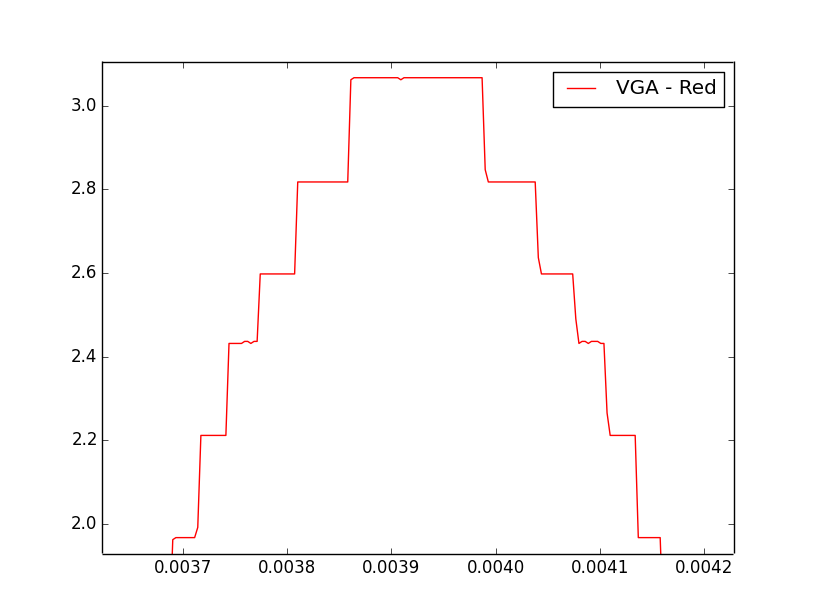
Once I had the system working, I looked at the sampled waveforms and noticed a problem: where it should have been flat, the red sinusoid had significant "bowing" at its peaks and troughs. Now what?
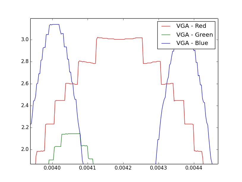
I thought this might be caused by some external interference coupling in through the wire loops connecting the VGA outputs to the ADC inputs, but changing the orientation of the wires or wrapping them with a ground wire didn't remove the bowing. In addition, the bowing was extremely consistent, always occurring in the same location and always by the same amount. That indicated it was caused by some signal generated by my boards and not by some external noise source. To get a better look at the distortion, I zeroed the amplitude and DC offset of the red sinusoid generator and took another sample:
This made it pretty clear that the blue signal was coupling into the red, somehow. I thought it might be crosstalk between the traces on the PCB, so I removed the wire carrying the green signal and grounded that input channel of the ADC board. This essentially put a guard wire between the PCB traces carrying the red and blue signals, which I hoped would absorb any crosstalk. Nevertheless, I saw no reduction in the bowing. I also noticed there didn't seem to be any coupling of the blue signal into the green signal, though the green trace on the PCB is even closer to the blue trace than the red trace is. So that seemed to eliminate crosstalk as the culprit, thus leaving me with nothing.
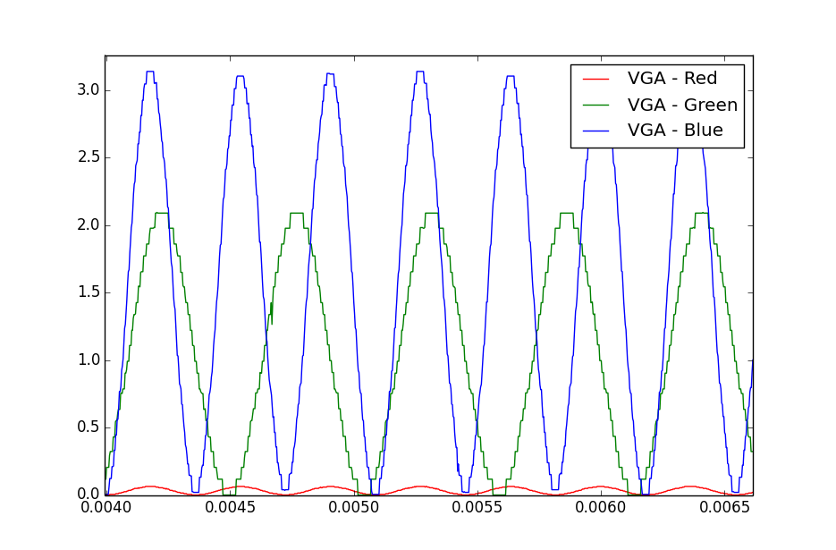
Finally, I started thinking about the sampling process itself. To sample multiple inputs, the ADC108S interleaves its sampling of the waveforms like so: red - green - blue - red - green - blue - ... The interleaving is done in the chip by switching an analog multiplexer feeding into a track-and-hold (T&H) circuit. When the blue signal was sampled, possibly it was leaving a remnant of itself in the T&H circuit that offset the sample value of the red signal that followed. To test this, I returned the signal generators to their original configurations but only sampled the red signal so the multiplexer never switched. The resulting waveform had no apparent bowing:
So the problem was caused by the multiplexer in the ADC chip. I looked for a possible solution in the ADC108S datasheet and found this:
Resistor R1 is the on resistance of the multiplexer and track/hold switch and is typically 500 ohms. Capacitor C2 is the ADC108S102 sampling capacitor, and is typically 30 pF. The ADC108S102 will deliver best performance when driven by a low-impedance source (less than 100 ohms). This is especially important when using the ADC108S102 to sample dynamic signals.
The output impedance of the StickIt! VGA board red, green and blue outputs is around 300 ohms, so that explained why there was cross-signal distortion. Placing unity-gain amplifiers on the analog inputs would lower the impedance seen by the ADC108S and solve the problem. Or just don't connect the board to high-impedance sources. Quite frankly, I'm starting to lean toward solution #2.
That's the current status of the ADC board. The KiCad and FPGA design files are stored on Github. My next task is to replace the LP2950 with an LP2980AIM5 in an SOT-23 package and have the board fabbed again. There goes another $14!
Share on Twitter Share on Facebook Share on Reddit
Comments
I hope this success means the Xula schematic & PCB will be re-done in Kicad format. Even better would be PDF versions - everyone seems to have a PDF reader these days.
Link / ReplyI'd like to add / modify a Xula-2 with an 80 MHz oscillator...
New Comment