![]() I made the decision last year to move from Eagle to KiCad. I got tired of releasing OSHW boards that many people couldn't modify because the freeware version of Eagle was so limited. I also got tired of paying $600 for upgrading to the next major release, especially when the big, new feature was ASCII-encoded design files. Really, that's it?! Hold me back!
I made the decision last year to move from Eagle to KiCad. I got tired of releasing OSHW boards that many people couldn't modify because the freeware version of Eagle was so limited. I also got tired of paying $600 for upgrading to the next major release, especially when the big, new feature was ASCII-encoded design files. Really, that's it?! Hold me back!
I got a taste of the KiCad design flow by watching Chris Gammel's "Getting to Blinky" video series while I was sitting in a hospital waiting room. Chris's videos made the time pass so quic ... nope, still bored. Though it was a better use of the time than folding and reorganizing the disposable hospital gowns. Damn you, OCD!
But eventually, as I learned in grad school, you have to stop reading stuff and start doing stuff. So last week, I downloaded and installed the latest development version of KiCad for Windows. (My philosophy is, if you're going to learn to drive, it might as well be on a car where the brakes don't work.) It takes a while to build KiCad, but having the source available can be important (as I'll discuss later).
As my first project, I decided to build a StickIt! module for an eight-channel ADC chip, the TI ADC108S. StickIt! modules are small (2.0" x 8") and usually only need a two-layer PCB, so I figured this would be easier than a four-layer PCB with a 256-ball BGA.
I used KiCad's Eeschema tool to enter the schematic shown below. It works pretty much like most schematic editors I've used. (However, I was never able to figure out how to globally rename a net; I had to click on each stub where the net name was used and rename it.) I also learned how to define new parts for the schematic because, as usual, the parts you need are never in the libraries. (I also checked at the KiCad CLoud parts repository. No luck.)
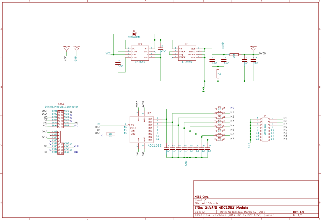
Going from a schematic to laying out the PCB isn't as seamless in KiCad as it is in Eagle. You have to:
CvPCB tool.PCBnew and import the netlist.There's also no live-link between the schematic and the PCB layout, so you can't highlight a net in the schematic and then see it in the layout. Still, it gets the job done.
The steps for using PCBnew aren't much different from any other layout tool:
PCBnew has these parameters spread around between the Dimensions and Design Rules menus, so it's kind of confusing.)PCBnew has a nice feature where all the air wires are hidden except those connected to the part you're currently moving.) There's an auto-placement feature as well, but I didn't find out about that until I finished the layout.Here's the front and back layouts for my first board:
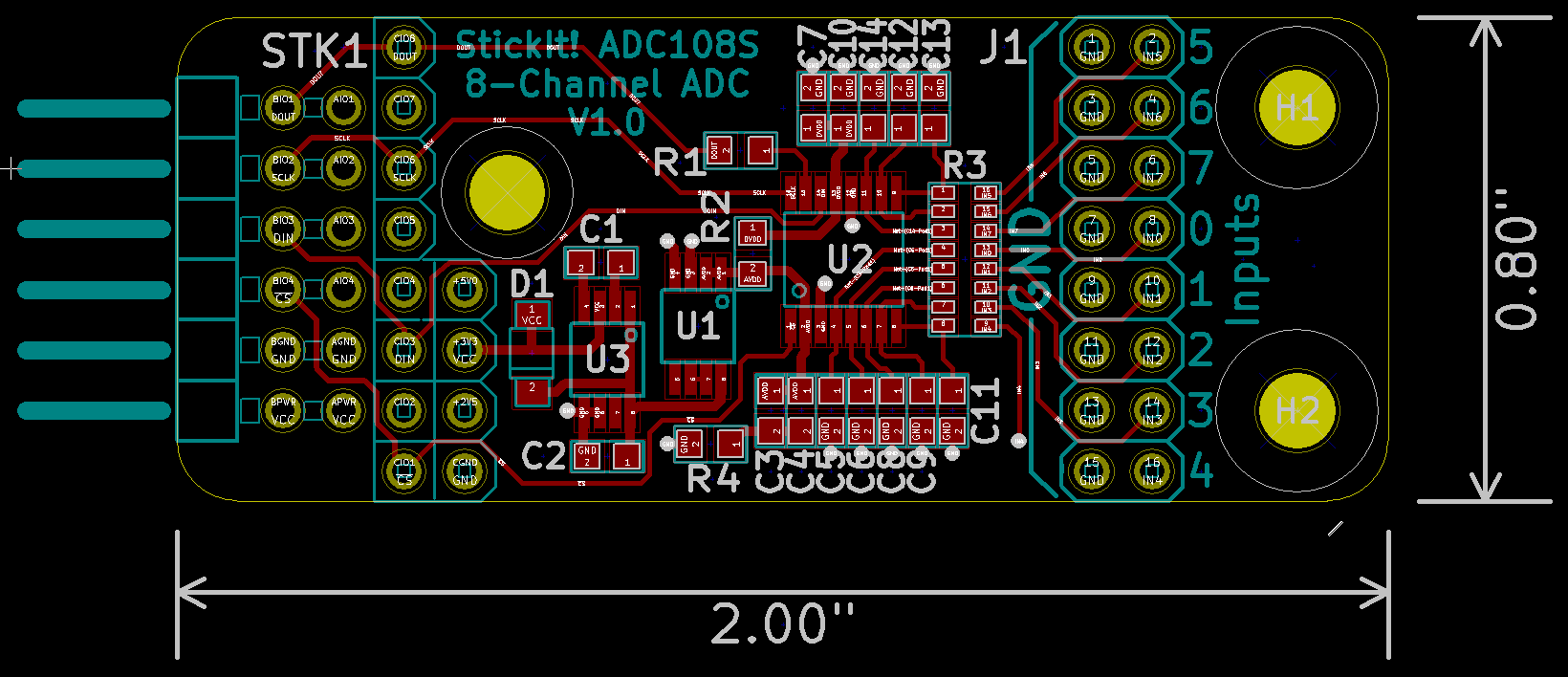
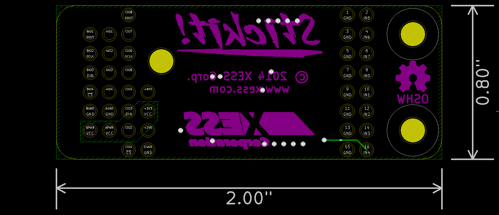
One of the pain points for the layout was, oddly enough, generating the graphics for the back-side of the PCB. KiCad provides the Bitmap2Component tool for translating any of around twenty different graphic file formats into a footprint you can place in a silkscreen layer. It produces a much smaller, easier-to-handle file than the equivalent tool in Eagle. But it's limited in that there's no way to scale the footprint: it uses a fixed resolution of 300 dpi, so if your image is 1200 pixels wide, it will be 4 inches wide on the board. I had to write a small Python script to scale all the polygon vertices in the .kicad_mod file that was generated by the tool. (It's nice that all the KiCad files are ASCII text and have well-structured formats that are easy to parse.)
I had a problem getting PCBnew to find the new footprint; it kept reporting "library module path does not exist." Since the error message was providing a .c file and a line number where the problem was found, I could check the source to see if I could find a solution. From that I was able to determine that I only needed to provide the directory for footprint files of type .kicad_mod and not the file itself.
Another problem was that when I placed the graphics footprint on the backside of the PCB, I was unable to mirror it. That meant the text would read backwards when the board was flipped over. I solved the problem by using a negative scaling factor for the X coordinate in my Python script. It was only while writing this post that I found I had to do the mirroring of the footprint in the Module Editor instead of PCBnew, but even then it doesn't seem to be working for me.
Once the layout was done, I generated the Gerber files for the PCB fabricator. (This function is under the File => Plot menu instead of the File => Fabrication Outputs menu where you can, however, generate the drill file. WTF?) I checked the Gerber files with the GerbView tool and also using the free version of ViewMate from PentaLogix. The results seem to match, but the Y coordinate-mapping translates the layout below the X-axis. I can't find a way to change that. I guess I'll see if that has any effect when the boards are made. At least the drills and the wire traces match up.
Now that the boards are sent for fabrication, how would I rate the whole experience? Good, overall. KiCad has its quirks, just like Eagle. (I think the designers of both must have attended Crazy Eddie's UX Design School.) In most cases, I think my problems were caused by inexperience and will lessen once KiCad gets into my muscle memory.
If I were starting to do PCB design from scratch today and needed to select a design tool, I would pick KiCad over Eagle. Here's why:
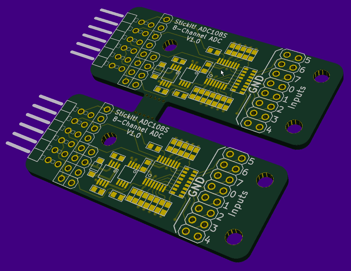
Besides, how can you not like a tool that gives you 3D board visualizations right out of the box!
Comments
Great article! I haven't done much with KiCad, and I'm looking forward to it maturing into a contender. It's good to have options.
Link / ReplyI agree completely with you on naming. We should have a tool-agnostic language, and resist this land-grabbing-empire-building crap that confuses everyone, especially those who're starting out.
Finally, isn't is remarkable, though, that a tool like KiCad is on par with a commercial tool like Eagle that has been around for so long? It tells us of the strides we're making in open source EDA development, but also about the abysmal disregard for user experience by commercial EDA tools all these years. I hope that they're paying attention!
New Comment