 I wrote a blog post several years ago about my first KiCad design: an eight-channel analog-to-digital StickIt! board. While testing it, I discovered the signals in the analog channels could leak into one another if the signal drivers had too high an impedance. The design kind of languished after that.
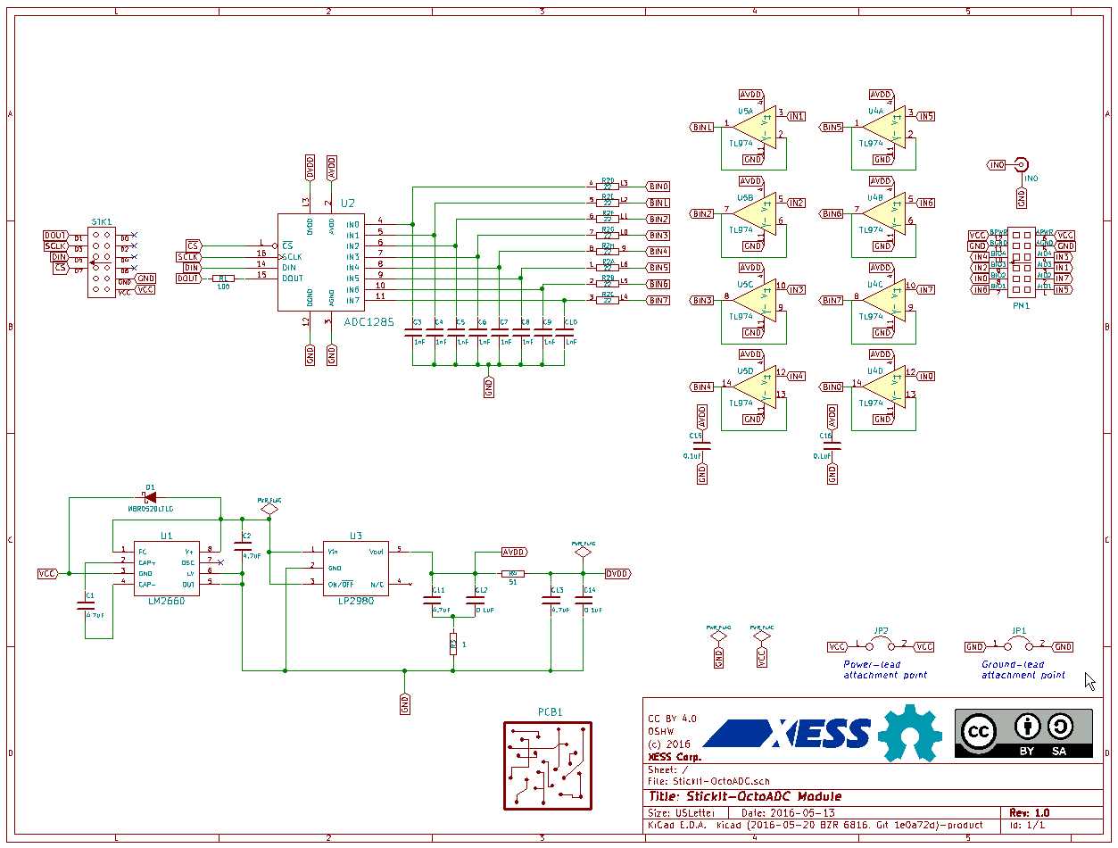
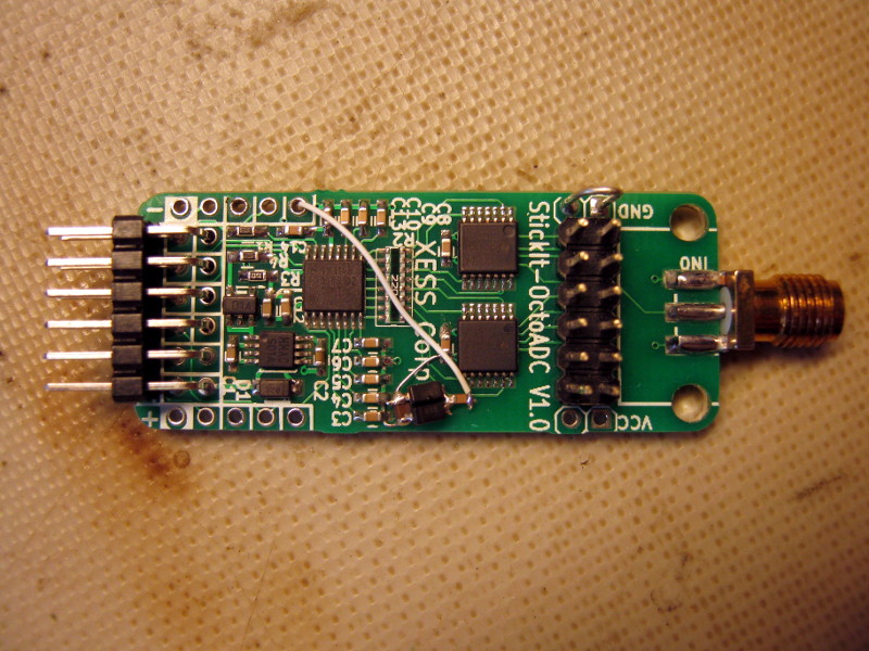
But a few months ago as I was building an array of StickIt! boards for fabrication, I decided to resurrect the ADC board (now called the OctoADC). I modified the design so the ADC inputs would be driven by dual quad opamps (TL974) with low-impedance outputs to stop the signal leakage. Here's the modified schematic:
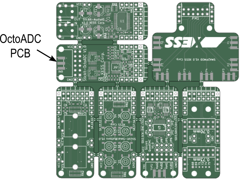
Eleven copies of the PCB array containing the OctoADC (and six other designs) were fabricated by dirtypcbs.com for $25.
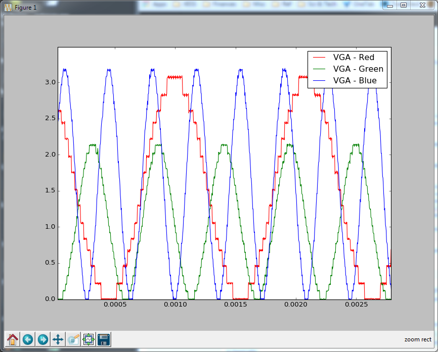
Upon receiving the PCBs, I assembled an OctoADC board and ran a test where it samples three, low-resolution sine waves (4-5 bits). These are the results I got:
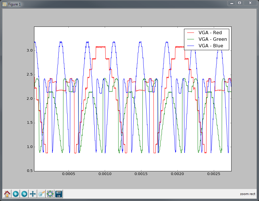
Yowsa! Definitely a turn for the worse!
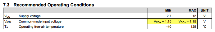
By looking at the waveform for a single channel, it became apparent that the sampled waveform goes nuts when the input drops near ground. It turns out I had mistakenly assumed the TL974 could handle an input voltage near ground (which I used as the negative rail) because they were described as "rail-to-rail" opamps. However, that only applies to the opamp output; the input has to stay at least 1.15 V away from either rail. (Doh! I really should start reading these datasheets.)
So my opamps needed at least a -1.15 V supply, but there's not a negative supply on the board. I had walked myself into a real mess and now I was going to have to to walk myself out of it.
My first thought was to use an LM2660 to generate a negative supply. But that chip is relatively expensive and the datasheet recommends placing another regulator on the output of the LM2660 to clean-up the noise. That seemed like a lot of added circuitry and expense for what I needed, so I decided to look for more "creative" options.
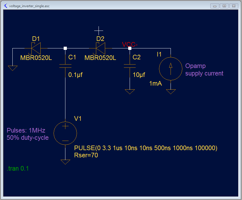
Taking a look at my existing design, one resource I did have was four unused I/Os on the PMOD connector that can be driven by the FPGA. From my beginning circuits classes I knew I could generate a negative voltage by applying positive pulses to a combination of diodes and capacitors like the circuit shown below. To test the idea, I modeled the FPGA pin in LTspice as a pulsed 3.3V supply with a 70-ohm series resistance, and I represented the current draw of the opamp with a 1mA current source.
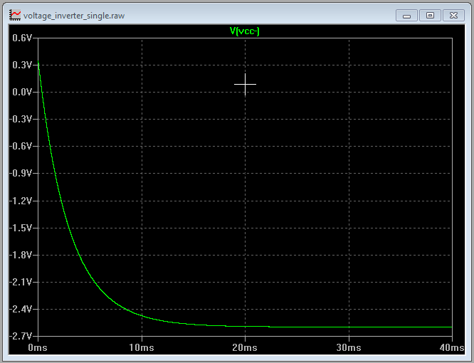
Simulation showed that, after an initial charging transient, pulsing the circuit with a 1 MHz square wave resulted in a stable negative voltage:
Due to their series resistance, the FPGA pins can't output an infinite amount of current. In combination with the current draw of the opamp, this limits the size of the negative voltage that can be generated. By varying the current source, I could plot the negative voltage that would result for various amounts of opamp supply current:
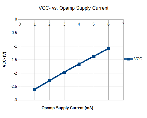
From the graph, it looks like I can draw no more than 6 mA from the negative supply before it fails to provide the -1.15 V the opamps need. The datasheet shows each opamp consumes 3.2 mA (worst case), so eight of them will require 25.6 mA. By combining four FPGA pins in parallel to decrease the equivalent series resistance, I thought I might be able to achieve that.
At this point, more accuracy was needed so I downloaded the Spice model for a single TL972 opamp. I placed the TL972.lib file in a local directory and used a .lib Spice directive to access it. I instantiated a single TL972 in a unity gain configuration with the non-inverting input driven by a 5 V, 10 KHz sine wave centered at 2.5 V. The positive rail of the opamp was fed by a 6.15 V source while the negative voltage generator feeds the negative rail.
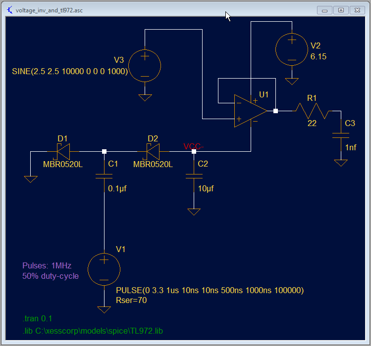
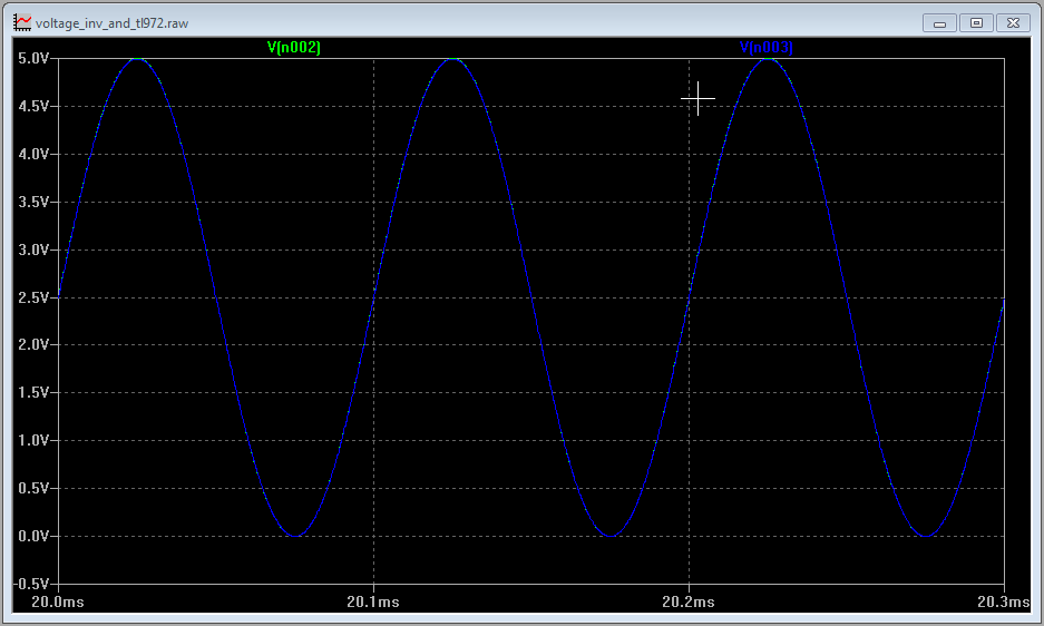
A simulation showed the opamp was working correctly as its output (the blue trace) exactly matched the input sine wave (the green trace). The output was also able to get to ground without any distortion.
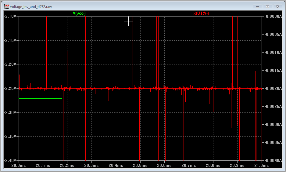
In addition, the negative rail current (the red trace) was only 2 mA (albeit with some substantial spikes) while the voltage (the green trace) was -2.27 V and free of noise.
Simulations are nice, but eventually you have wire together some parts and make it work in the real world. So I drew up a component layout for the negative voltage generator (otherwise I'd end up wiring it wrong):
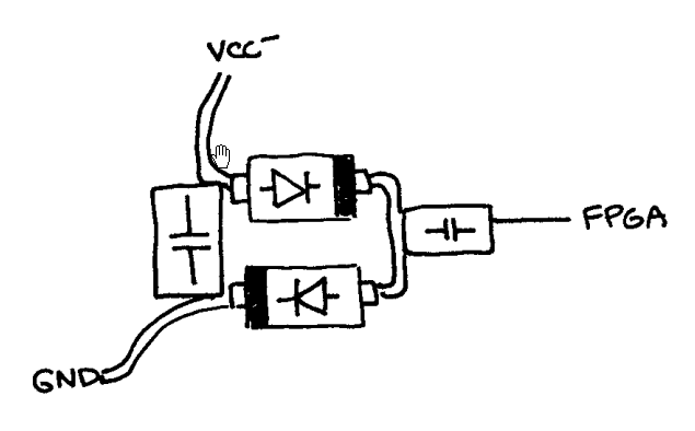
And then I soldered it onto the OctoADC board (which is even uglier than the drawing):
Once the hardware modifications were complete, I modified the FPGA design to include a pulse-width modulator (PWM) that outputs a 1.5 MHz square wave. The PWM signal exits the FPGA on up to four pins to drive the negative voltage generator, but I found in my experiments that using three outputs was enough to generate a stable -2.7 V supply rail. (Obviously, my modeling of the FPGA outputs as a voltage source with a 70-ohm resistor was too conservative.)
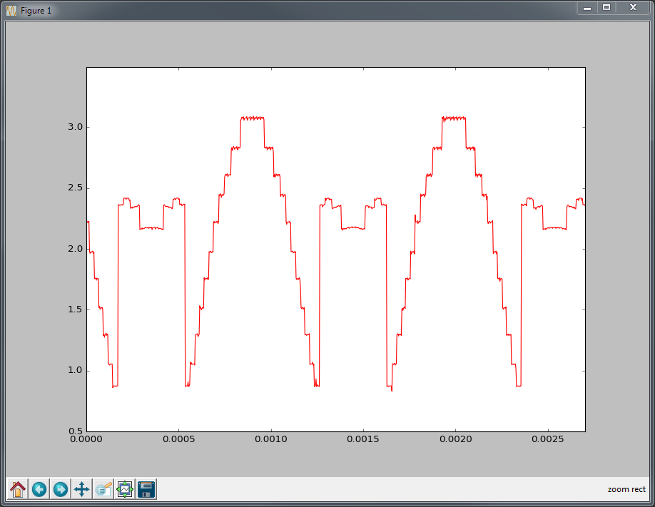
When I re-ran the test with the modified OctoADC board, the results were much better. Now you can clearly see the three, separate quantized sine waves.
So I managed to walk (crawl?) my way out of my current problem. Now it's just a matter of modifying the OctoADC PCB and including it in my next array. And then on to the next problem...
Share on Twitter Share on Facebook Share on Reddit
Comments
New Comment