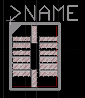
Making footprints and schematic symbols are some of the more onerous parts of using Eagle. But most ICs are pretty similar: they're either DIPs, some type of leaded SMD, or BGAs. So I made a Perl library that lets me enter a simple text description of a chip and it will generate a footprint and symbol for me and link them together into a complete device.
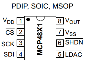
As an example, consider the Microchip MCP48X1 DAC chips. Here's their pinout:
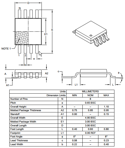
And here's their footprint:
Here's how I describe the MCP48X1 using my library:
use make_eagle_lib; # Import the Eagle part-making library.

print make_symbols(); # Instantiate the schematic pin symbols.

# Create a leaded SMD package footprint.
print make_qfp_pckg(
    # Create the footprint name, title and description to display in the Eagle library.
    name           => 'Microchip-8_MSOP',
    title          => 'Microchip 8-Lead Plastic Micro Small Outline Package',
    desc           => '',   # Description of package.
    # The rest defines the actual footprint.
    units          => mm,   # All units are in millimeters.
    contact_width  => 0.4,  # Lead width. (Dim. "b")
    pad_width      => 0.4,  # Pad width. (Dim. "b")
    # Total pad length = contact_length + back_porch + front_porch.
    contact_length => 0.8,  # Foot length. (Dim. "L")
    front_porch    => 1.0,  # Outward extension of pad.
    back_porch     => 0.0,  # Inward extension of pad.
    pad_spacing    => 0.65, # Lead pitch. (Dim. "e")
    num_pads_x     => 4,    # Number of pads along the horizontal sides (MSOP package).
    num_pads_y     => 0,    # Number of pads along the vertical sides.
    chip_x         => 3.0,  # Overall length. (Dim. "D")
    chip_y         => 4.9,  # Overall width. (Dim "E")
    add_fiducials  => 'no', # Don't add fiducial marks for placement.
);

# Create the device that uses the footprint.
%device = (
    # Create the device name, title and description to display in the Eagle library.
    name  => 'MCP48X1',
    title => 'Microchip MCP4801/4811/4821 DAC',
    desc  => 'Microchip 8, 10 and 12-bit DACs with SPI interface.',
    # Now link the footprint with the device.
    pckgs => [
        {
            name       => 'Microchip-8_MSOP', # Footprint name from above.
            variant    => '-E/MS', # Package variant label (could be '' if only one footprint).
            num_pads_x => 4, # Same number of pads as above.
            num_pads_y => 0
        },
    ],
);

# Create the device pins.
%pins = (
    default_swap_level => 0, # By default, pins are not swappable.
    properties         => {
        # Specify the name and I/O type for each pin of the device.
        1 => { name => 'VDD',   type => IN  },
        2 => { name => 'CS#',   type => IN  },
        3 => { name => 'SCK',   type => IN  },
        4 => { name => 'SDI',   type => IN  },
        5 => { name => 'LDAC#', type => IN  },
        6 => { name => 'SHDN#', type => IN  },
        7 => { name => 'VSS',   type => IN  },
        8 => { name => 'VOUT',  type => OUT },
    }
);

# Now combine the device and pin descriptions into a complete device.
print make_device( device => \%device, pins => \%pins );
Assuming the part description is contained in a file called my_part.pl, I can make a script file for the part using the command:
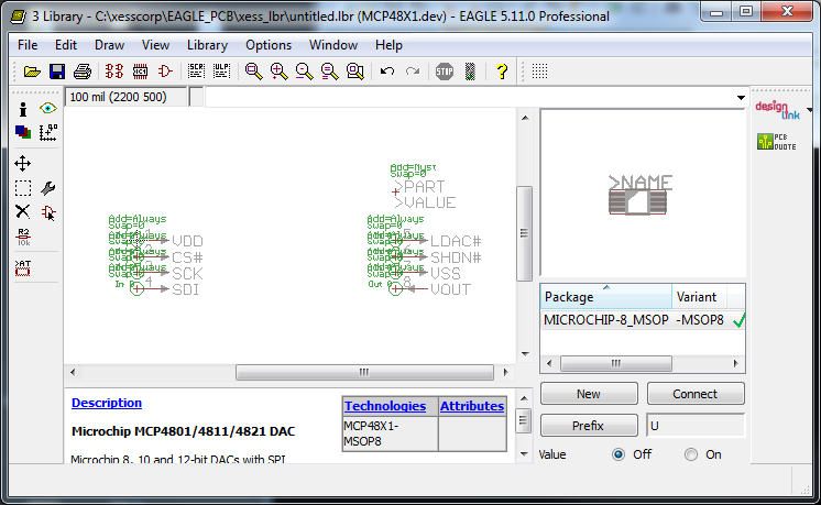
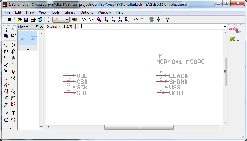
perl my_part.pl > my_part.scrThen I start Eagle, open a library where I want the part to reside, and excute the my_part.scr script. Here's the resulting device view:
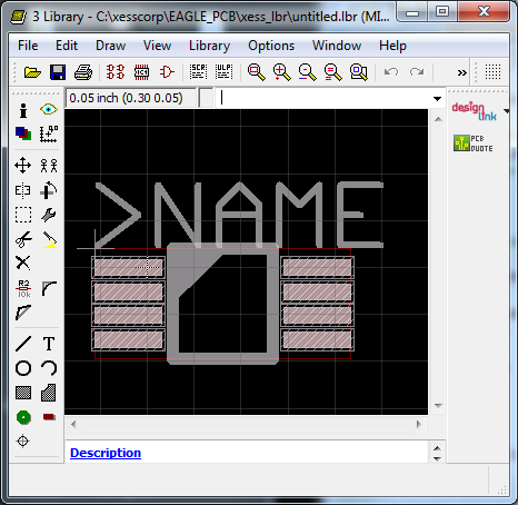
And this is the footprint:
The schematic symbol is a bit different from what most people are used to. Each pin is actually defined as a gate and you can arrange them any way you want.
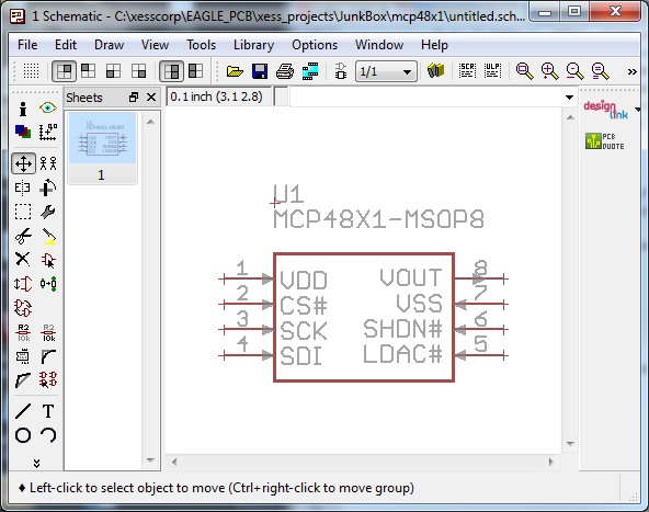
I usually arrange them to look like the actual package and then draw a boundary around them:
But I know others like to arrange them functionally:
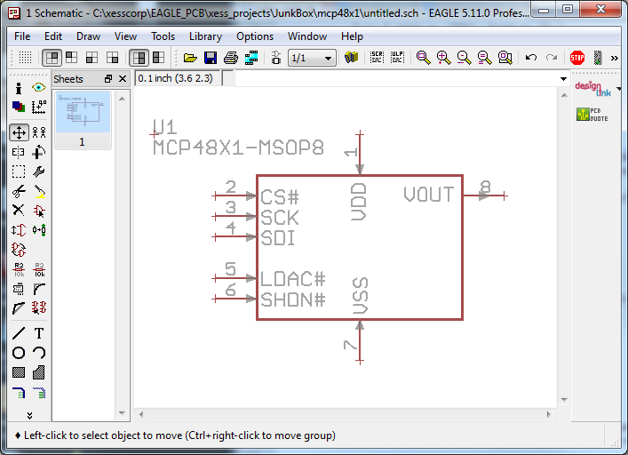
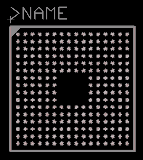
The advantage is the pins can be arranged in whatever manner makes sense to you (and everyone seems to have a different opinion about that). This is a particular advantage when you have to deal with high pin-count packages like 256-ball BGAs. The disadvantage is you can't just pick up the entire part and move it around; you have to select all the pins as a group first and then move it.
So why use this perl libray instead of doing it manually or by using a ULP that helps you define a single device?
When would you not use this perl library? Basically, I don't use it when I come across some funky footprint with odd pad arrangements and/or oddly-sized pads. MicroSD cards and some semiconductor power devices spring to mind. For these, it's usually best to do it manually.
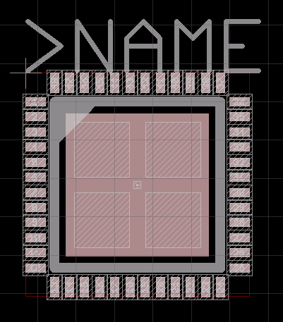
You can download my Eagle part maker library from github along with some example files for various DIP, leaded SMD, and BGA devices. Here's some examples of the footprints I've built with it. These footprints all took minutes to create and required no manual tweaking. The most time-consuming task is manually entering the list that associates the schematic pin names with the footprint pads.

Comments
New Comment