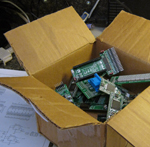
 When I demoed a few projects at the recent Maker Faire NC, I also brought along a loose box of projects for people to paw through. (The little kids loved 'em. Nothing puts out an eye like an 0.1" header.) Most of the stuff was old XuLAs and StickIt! motherboards and modules. But the one most people asked about was just an unpopulated PCB I'd designed back in 2011 and had never gotten around to doing anything with. (That's one of the unexpected consequences brought on by companies like Itead: you can make a PCB for a project and, because it's so cheap, you don't care if you never finish it.)
When I originally designed the XuLA in 2010, it was with the intention of making a cheap logic analyzer with a deep buffer (2M x 32). That's why it has 33 I/O pins: 32 for data inputs and one for a clock strobe. (That cost me dearly, too. I had to give up half the capacity of my SDRAM because the FPGA didn't have enough I/O left over for both bank-select pins.) While doing the PCB, I decided the XuLA would make a good, general-purpose, FPGA dev board and started moving in that direction.
About a year later in June of 2011, I returned to the logic analyzer idea. I knew it would be too difficult for people to attach probe leads to an unmodified XuLA, and even then it would only be able to sample signals from 3.3V circuits. So I designed a motherboard that would bring the XuLA I/O pins out to a convenient header through some logic-level translators. That's the PCB the people at Maker Faire were looking at.
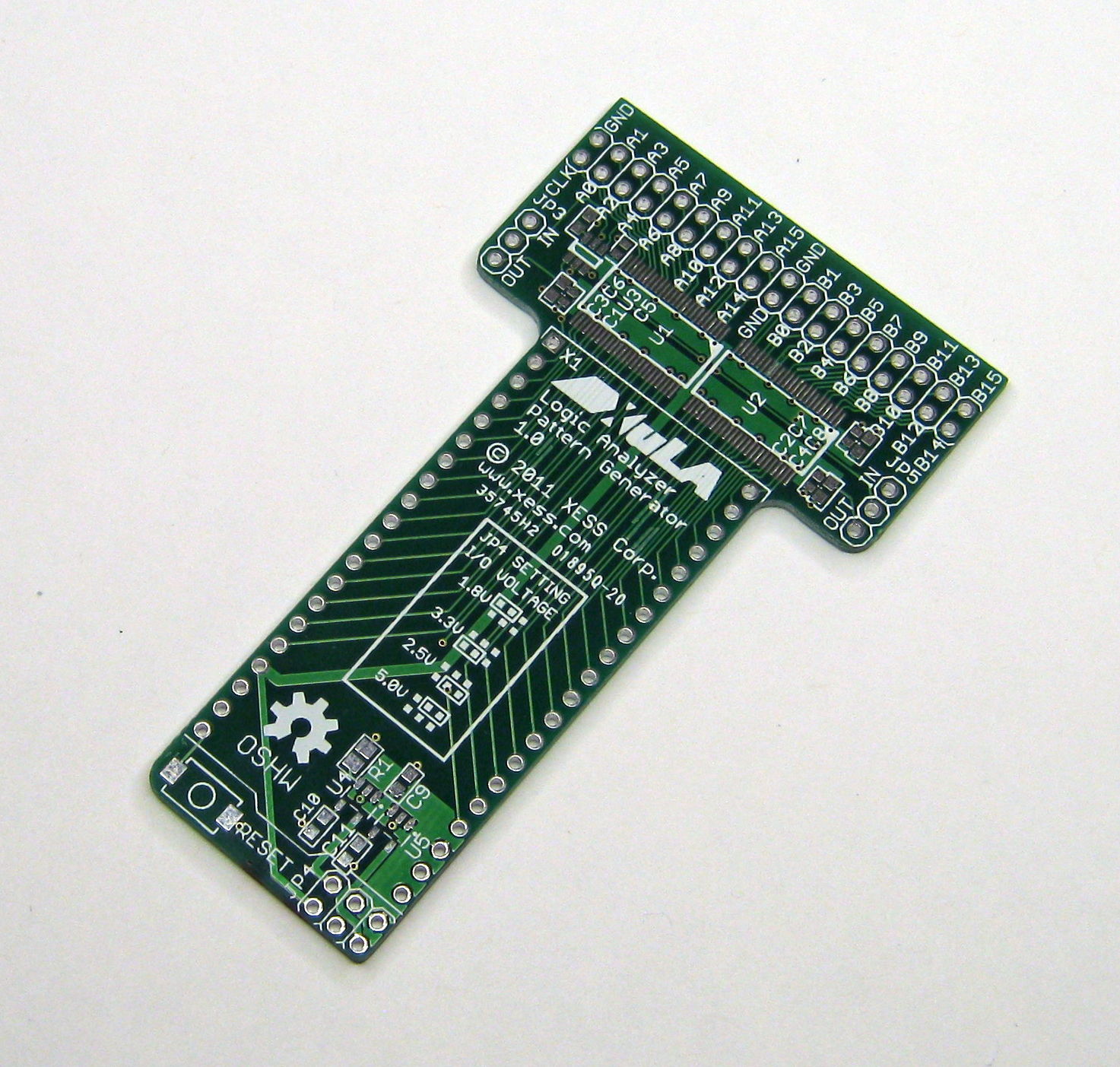
Located near the 36-pin header for the logic probes are a pair of 74LVCH16T245 translators, each one capable of translating 16 signals. Then there's a 74LVC1T45 for handling the one remaining signal, for a total of 33. The 33 signals are divided into two sets: the A-side with 17 signals, and the B-side with 16. Each side has a jumper that selects whether its signals are inputs coming from the outside world into the XuLA board, or outputs driven by the XuLA board into the outside world. (That lets me use the board as a digital pattern generator or as a half logic analyzer / half pattern generator.)
At the bottom of the board (near the RESET button) are a pair of voltage regulators. These create 1.8V and 2.5V supplies in addition to the 5V and 3.3V supplies already output by the XuLA. By placing a shunt on the JP4 jumper, one of these four supplies is connected to the logic-level translators. This adjusts the 3.3V I/O of the XuLA so it can transfer signals to/from systems built with 1.8V, 2.5V, 3.3V or 5V logic.
Since somebody showed some interest in it (and, hey, that can be a rare thing), I decided to finish building the prototype.
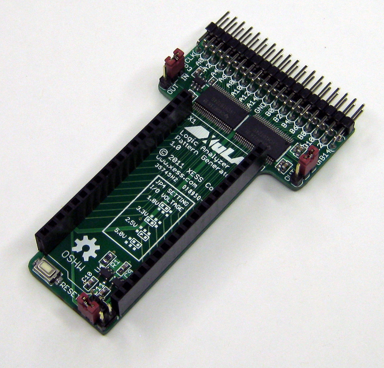
Here's what it looks like after I plug a XuLA board into it:
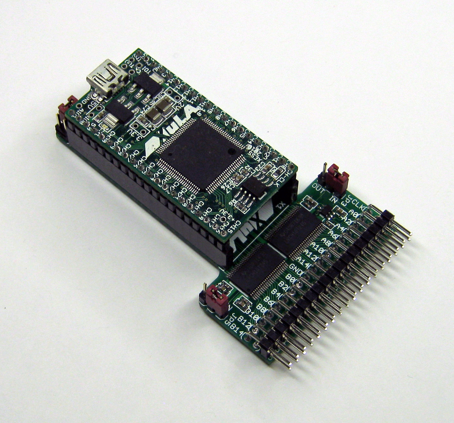
And, finally, with some probe cables attached:
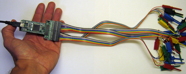
That's where I am right now. The current state of the project is stored here. As I get time, I'll start to map a current version of one of the open logic analyzers to the XuLA.
Comments
New Comment