 Sometimes things go well. And then they don't. And then you have to improvise.
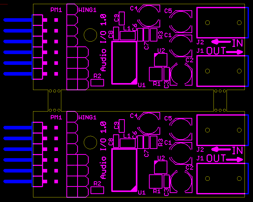
I had a 5cm × 5cm panel containing two boards connected by a break-away tab. Itead had previously fabricated this for me. When I submitted the Gerber files this time, Itead rejected it because the tab connecting the two boards was too thin. They recommended using a 10mm tab.
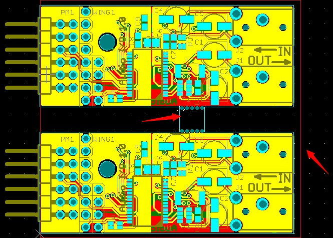
So I widened the tab and resubmitted the panel. They rejected it again, saying that I could not have so many drill holes so close together.
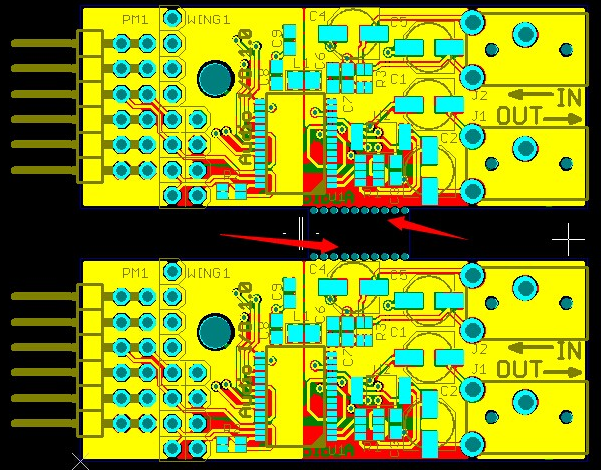
So I replaced the single tab with two, thinner tabs spaced further apart. Itead rejected it again:
Here are sub-board in your panel, but the slot between them is not pernitted.
Also please increase the coonection between them to at least 1 cm.
Obviously, there's no getting anything past them!
At this point, it looked like I would have reduce the panel to a single instance of the board in order to have Itead fabricate it. But Itead charges $9.90 to make ten 5cm × 5cm panels regardless of how much of the panel I use. So now I was only going to get ten individual boards whereas I was getting twenty boards in previous orders. Since I use Itead to get small runs of boards for low-volume products, this would essentially double my PCB costs.
So I decided to give Seeed Fusion PCB service a try. They have the same deal as Itead: ten 5cm × 5cm panels for $9.90. Seeed uses an automated system that scans your Gerber files upon order submission and then assigns the panel size depending upon your dimensions. In my case, Seeed's system came up with a panel size of 10cm × 5cm, even though my panel fits into a 5cm × 5cm area.
So I contacted Seeed's customer support and said "what's the dealio, yo?" (No, I didn't really say that.) They replied:
We make the board size according to the outline, the part out off the outline may be cut off. So please make sure all the layer are in the outline.
Well, the panel outline as defined in my .GKO Gerber file did fit in the 5cm × 5cm area.
However, my top-level silkscreen didn't; some of the part outlines overlapped the edges of the panel.
Maybe Seeed was actually looking at more than just the .GKO file?
To test this, I did a trial submission of my Gerber files with the silkscreen layers omitted.
Sure enough, the Seeed system assigned it to a 5cm × 5cm panel.
Now the question was how to eliminate the silkscreen overlap? Some of the overlap was caused by part outlines with features that should have only appeared in the documentation layers (which aren't fabricated) instead of the silkscreen. I could fix those in the libraries and re-import the parts into the original PCB layout, but then I would have to rebuild the array and put in the connecting tabs, etc. That seemed like a lot of work. Plus, it wouldn't fix the overlaps caused by part outlines that actually were supposed to be on the silkscreen (such as connectors at the edges of the board).
The next option was to edit the Gerber files directly and clip-off the overlaps in the silkscreen layer. I check my Gerber files using a free program from Pentalogix called ViewMate and it also allows editing. However, it doesn't allow you to save the edited files. Pentalogix will sell you a program called ViewMate Deluxe which does that. For $95.
Well, I didn't want to pay $95 for a program that I only needed to clip-off some silkscreen. Plus, I would need to use it manually on any board that had an overlap. I don't want to do things manually. I live in the future, where everything is automatic!
So I went looking for something that was free and/or open-source to do this for me. I mean, this isn't some esoteric procedure that only I would want to do, right? However, the programs that were out there either didn't do editing, had a funky user interface, or wouldn't run on Windows.
But then I found pcb-tools. This is a Python module for handling Gerber files. It seems to be mainly geared for displaying Gerber files. But right off the bat, it handled getting the bounding box of a layer. How hard could it be to modify the code to clip-off elements that went outside a given bounding box?
Well, it was a little harder than I thought. I had to recall how to clip a line segment against a bounding box from the computer graphics course I taught 25 years ago. Then there were those little edge cases (literally) where the endpoints of segments ended up right on the edge of the bounding box. But, eventually, I got it working. Here's the result for my board as seen with ViewMate:
The original silkscreen with the board outline. Notice the overlap.
The clipped silkscreen with the board outline. No more overlaps.
The original silkscreen superimposed with the clipped version. The magenta shows where they coincide. Notice that only the part of the silkscreen outside the bounding box has been removed.
Using my new program, I was able to clip my silkscreen layer and resubmit my panel to Seeed. They accepted it with a panel size of 5cm × 5cm. Success!
Share on Twitter Share on Facebook Share on Reddit
Comments
Seeed also includes the width of lines on the outline layer when calculating board size. I have always assumed that the centerline defines the board geometry. They fabricate boards with square corners, not the rounded end of the lines.
Link / ReplySeeed also calculates the board size using the outside dimension of the outline layer (unless some other layer is larger). I have always used the centerline to define board geometry. What possible information is conveyed in the trace width of lines on the outline layer?
Link / ReplyDave,
Link / ReplyPerhaps you should go back to itread. Just checked prices and quanity 5 30cm x 30cm 2 layer boards is $0.20!!!!
George
Hey, George. Haven't been able to find that offer. Got a pointer to it?
Link / ReplyNew Comment