XESS Boards have had built-in VGA interfaces since 1997 (and I stole the idea from others who were doing it before that). But the new XuLA FPGA board doesn't have any extraneous parts (just an FPGA, SDRAM, configuration flash and a USB interface), so how do you display graphics with it?
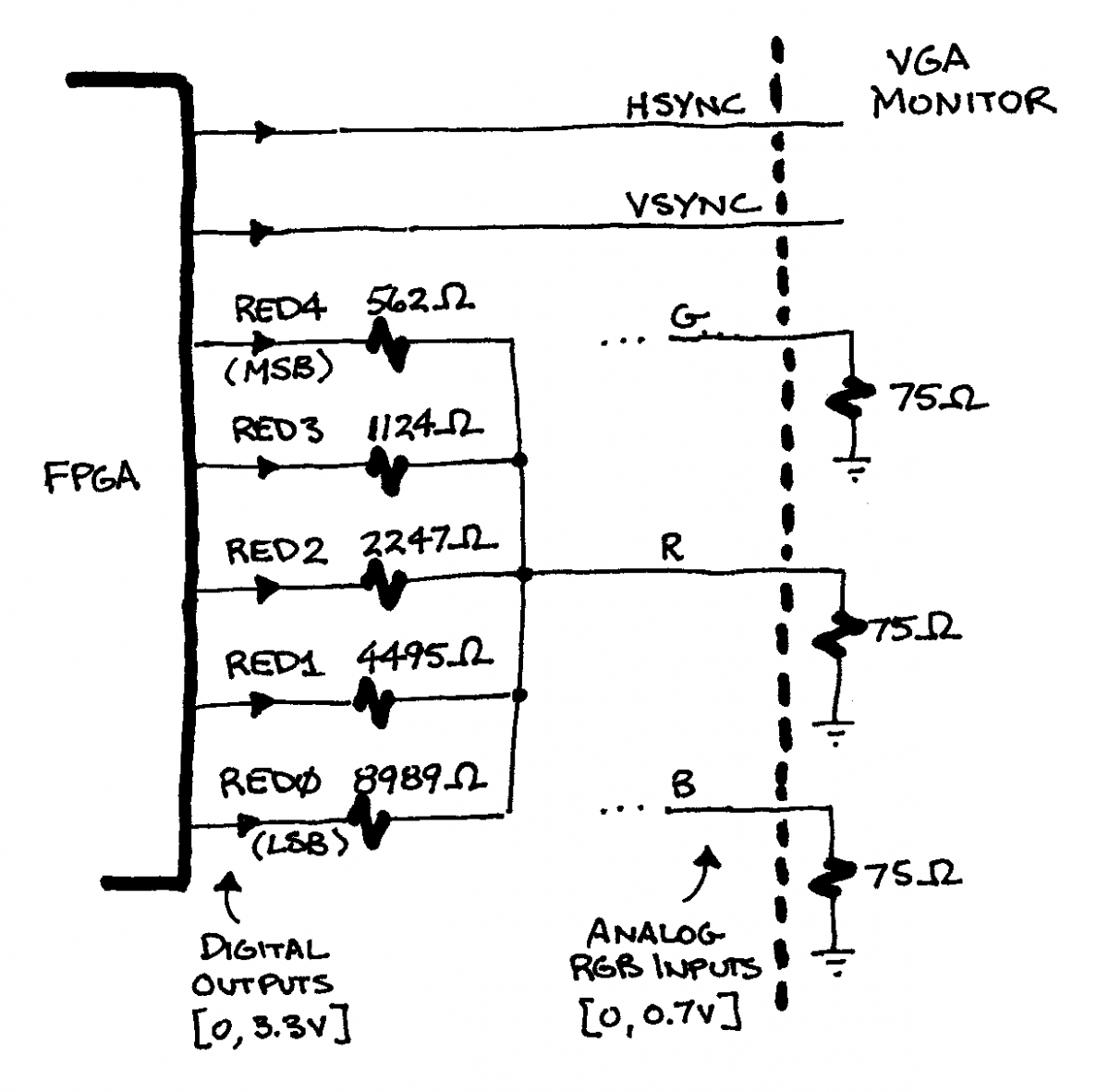
A simple VGA interface can be built on a breadboard with some resistors and a connector. The red, green and blue VGA signals are each driven by a simple DAC like the one shown below. Each color input presents a 75-ohm load to the DAC. The DAC resistors combine with the load resistor to divide the 3.3V digital logic outputs so the total stays below the maximum 0.7V expected by the VGA input. A set of five resistors that scale upwards by a factor of two will implement a single five-bit, 32-level DAC, so fifteen resistors are needed to drive the RGB inputs to create a total of 32 x 32 x 32 = 32,768 colors. Two additional digital outputs are needed to drive the active-low horizontal and vertical sync signals. So a total of 17 outputs are needed from the FPGA to drive a VGA monitor. (Of course, you can reduce the number of FPGA pins by reducing the number of color levels. For example, a simple black/white VGA display only needs a single resistor and three output pins.)
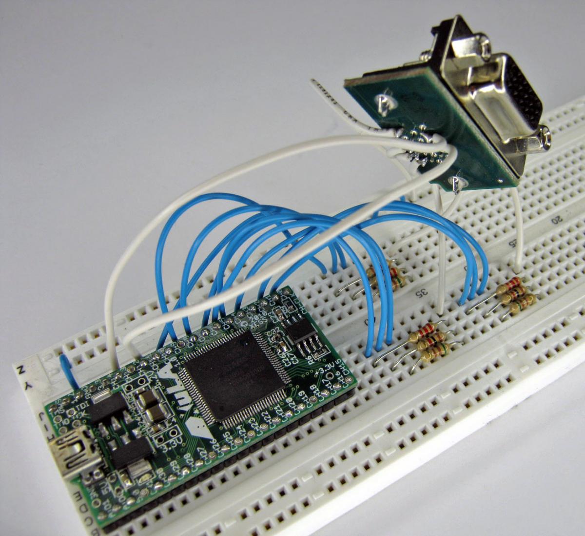
That's all good in theory, but the practical result is messy. Shown below is what a smaller 8 x 8 x 8 = 512-color VGA interface looks like. Only three resistors are needed in each DAC, and a total of eleven wires connect the VGA interface to a XuLA board. Then the DAC outputs, sync outputs and signal ground have to be soldered to a VGA connector (which I sawed off of an old XSA-3S1000 board). It's not that bad to build this once, but you wouldn't want to develop VGA apps if you had to rig this up every time.
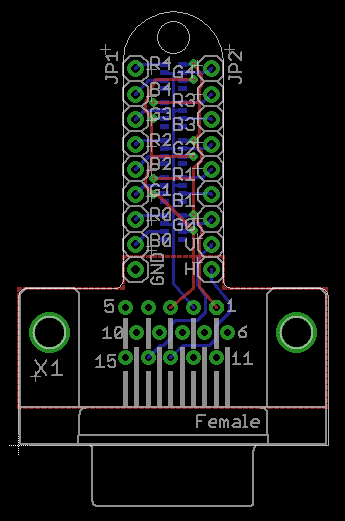
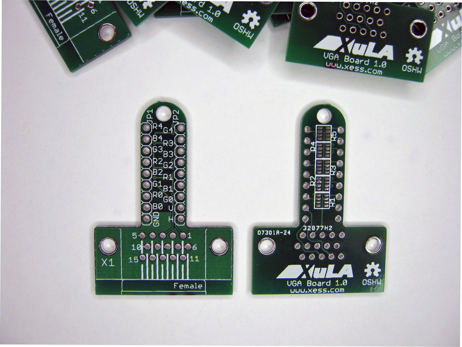
To reduce the drudgery, I designed a small, two-layer, 8/8-mil trace/space PCB that integrates the resistors and VGA connector into a form that can be plugged into a breadboard with 0.3" spacing. I submitted the Gerber files to ITEADstudio and I received the following PCBs eighteen days later (five days for fabrication, thirteen days by mail to North Carolina, USA). Total cost for ten PCBs + shipping: $16.
Here's an assembled VGA board and what it looks like connected to a XuLA board.
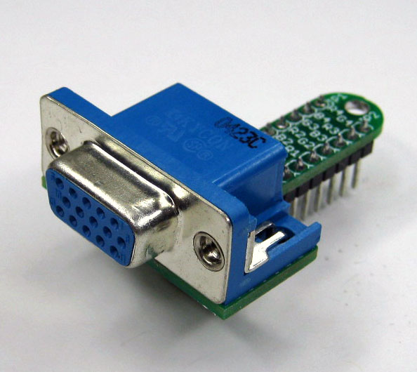
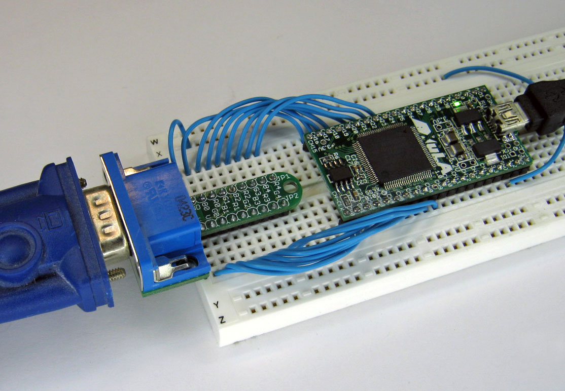
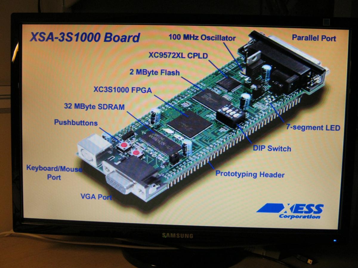
And here's a photo of some VGA output generated by this board. I loaded the SDRAM on the XuLA board with an 800 x 600 image that the FPGA continuously reads and displays on a monitor through the VGA interface. I couldn't use the exact DAC resistance values when I assembled the board because the resistor arrays only come in a limited number of values, but this doesn't seem to cause noticeable distortions in the displayed colors. (The Moire pattern you see in the picture doesn't appear when viewing the actual image on the monitor. It's caused by aliasing between the monitor's spatial screen resolution and the image resolution of my camera.)
Overall, I'm happy with the results I can get with this low-cost board. The only change I plan to make is to widen the board from 0.3" to 0.5" so the resistor arrays can be placed on the top side of the PCB while still leaving room to label the pins.
You can find the Eagle 5 design files for this board here. If you have it fabricated at Itead, then you might want the CAM and DRC files as well.
Comments
where is the zip file ?
Link / ReplyThis post is almost four years old. The files have drifted around a bit as I've switched web hosts. I revised the text and added the links to the Github repositories for the board files.
Link / ReplyNew Comment